
Flexible Silicon
A new approach
Ninety percent of today’s electronics are made of silicon. The semiconductor industry has billions of dollars’ worth infrastructure used to make our reliable and advanced electronics based on standard tools and processes that have been developed over decades of hard work and research. Still we do not have a matching enterprise for making tomorrow’s flexible and free form electronics. Therefore, we use various traditional and non-traditional fabrication processes and techniques to (i) build new flexible devices, (ii) transform existing bulk devices into flexible form. The processes we use are CMOS compatible.
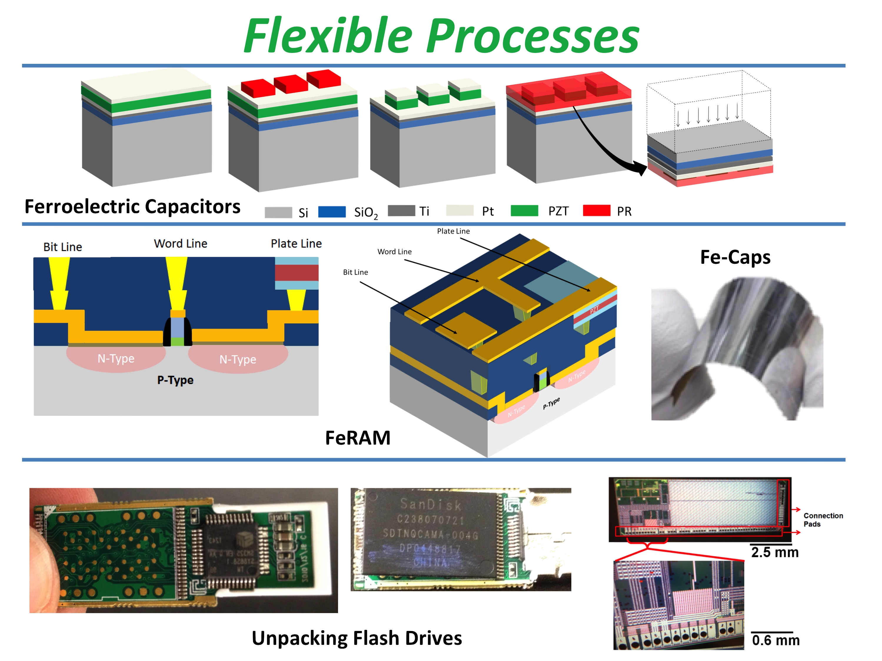
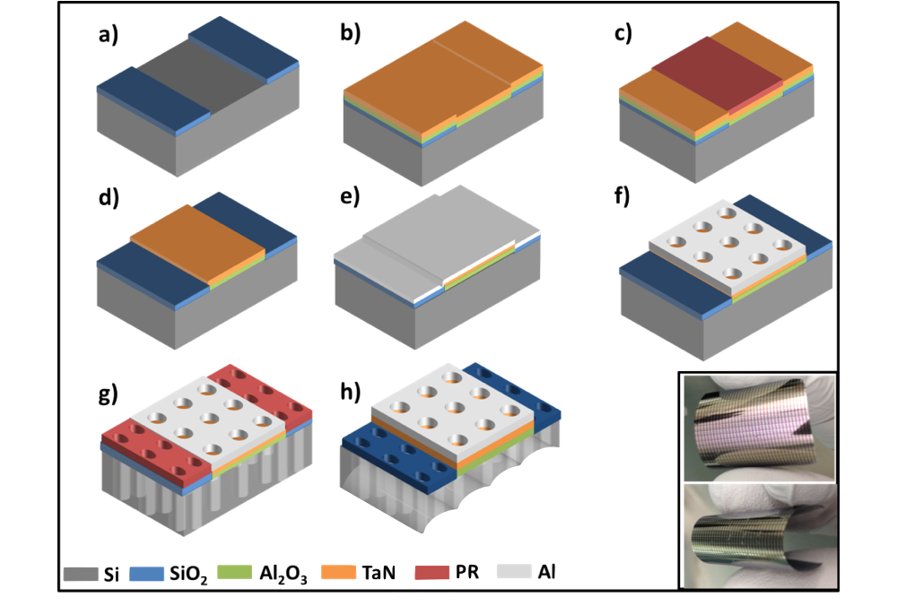
This means we can capitalize on the existing standard processes and existing infrastructure to make high-performance flexible electronics. We have built flexible versions of most commonly used ferroelectric lead zirconium titanate (PZT) capacitors in FeRAM, flexible metal-oxide-semiconductor capacitors (MOSCAPs) for DRAM and studying gate stacks, metal-insulator-metal capacitors (MIMCAPs) sued in DRAM, memristors for non-volatile memory applications and transformed state-of-the-art fin-field-effect-transistors (FinFETs) used in today’s fast powerful processors into flexible form.

“We have developed integration strategies for making high-performance flexible electronics, capitalizing on complementary-metal-oxide-semiconductor (CMOS) technology.”
We used a backside deep reactive ion etching (DRIE) process to reduce the thickness of a silicon-on-insulator (SOI) substrate bearing CMOS FinFETs and gain flexibility. This process is based on the strong inverse proportionality between the flexural modulus of a material and its physical thickness. The less thickness the more flexible the material becomes. This is similar to the fact that an aluminum rod is inflexible but Aluminum foil is flexible.Another approach to building CMOS flexible electronics we use is the etch-protect-release approach. This technique utilizes deep trenches (few to tens of micrometers) patterned in the unused area of a chip. These deep trenches are first etched, and then their sidewalls are protected. The final step in this process (the release step) is complete when an etchant gas passes through the bottom of the trench (the only unprotected region on the chip). The gas then etches the bottom of the trenches, creating growing spherical empty spaces at the bottom of the trenches. As time passes, the spheres grow bigger until the point where these spheres merge with spheres resulting from neighboring trenches. Then, a thin flexible layer of the fabricated chip bearing the devices is released (detached from the bulk substrate).
So where to from here then?
We have demonstrated flexible versions of various CMOS electronic devices for logic and memory applications. The devices performance was preserved to a great extent, even at small bending radii, and bending effect has been assessed and explained. Future works in that direction would be to demonstrate fully functional flexible systems that match today’s rigid state-of-the-art systems and have flexibility and free-form as an added feature.
Drop on in
4700 KAUST, Ibn Sina Building (3),
Thuwal, Makkah
Saudi Arabia, 23955-6900
Give us a call
Office: +966-2-808-4450
Lab Phone: +966-2-808-0797
Contact online
Email: MuhammadMustafa.Hussain@kaust.edu.sa
INL: nanotechnology.kaust.edu.sa