Silicon NanoTube FET
A new approach
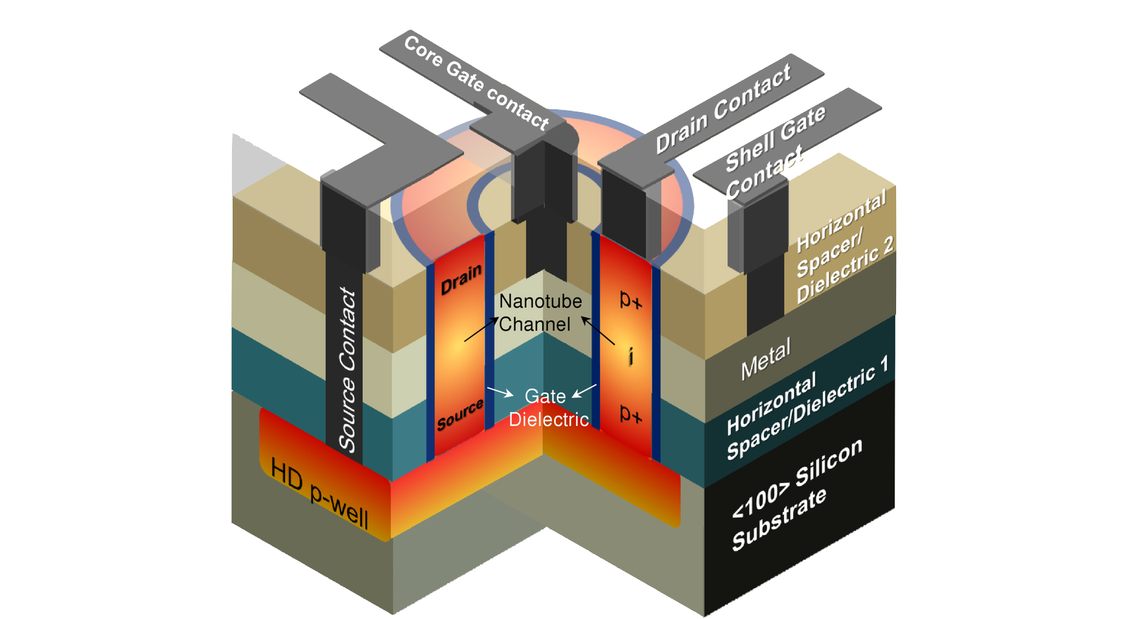
The novel architecture should maintain similar channel electrostatics to the GAA NW architecture to mitigate short channel effects, and thus allow channel length scaling-down. Also, a bottom up integration of the NT FET enables: (i) Growing intrinsic undoped channel using chemical vapor deposition based epitaxy (bottom-up) for better control of source/channel/drain properties. (ii) Formation of ultrasteep source/drain junctions in Si NT FET will be through in situ heavy doping during bottom-up epitaxial growth. (iii) Aggressive scaling short channel (Lg) by deposition thickness controlled gate length definition without any pre or post etch processing. (iv) Flexible choice of channel materials and its orientation
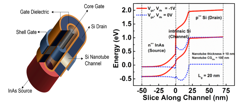
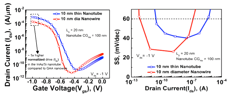
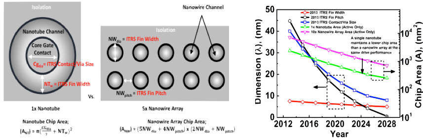
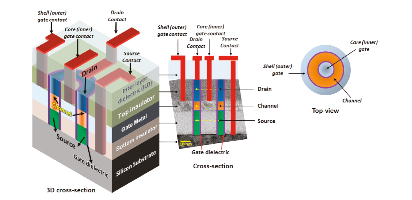
The core-shell gate architecture provides the following advantages when compared to the gate-all-around nanowire (GAA NW) MOSFET architecture (the competing future technology for beyond the 7 nm node): 1) Superior short channel effects control. 2) Ability to scale the ‘ON’ current value by controlling the core gate diameter without the need to array devices to achieve a high ‘ON’ current. 3) Higher Ion/Ioff. 4) Superior Area efficiency. 5) Superior Tunnel FET performance due to larger cross-sectional tunneling area. 6) Better scalability for future technology nodes.
“The objective of the project is a CMOS-compatible vertical device architecture that is able to provide superior performance to the contending gate-all-around vertical architecture in terms of drive current scalability, area efficiency, and thus integration density.”
Bottom up integration challenge would be achieving steep junction using non-metal catalyzed selective epitaxial growth in nano-sized trenches, as well as, forming good Ohmic contacts in vertical devices. Also simulation of NT FET based CMOS inverter/ring oscillator with the objective of optimizing parameters such as: channel length, channel thickness, and contact resistance effects should be attempted using Synopsys Sentaurus small-signal AC analysis module.
So where to from here then?
Studying the architecture advantages for both SRAM, and SONOS nonvolatile memories.
Drop on in
4700 KAUST, Ibn Sina Building (3),
Thuwal, Makkah
Saudi Arabia, 23955-6900
Give us a call
Office: +966-2-808-4450
Lab Phone: +966-2-808-0797
Contact online
Email: MuhammadMustafa.Hussain@kaust.edu.sa
INL: nanotechnology.kaust.edu.sa