
Silicon-Tin
A new approach
In this project, we present a novel semiconducting material, silicon-tin (SiSn), as channel material for complementary metal oxide semiconductor (CMOS) circuit applications. The material is an alloy of two group IV(a) elements of the periodic table, namely silicon (Si) an tin (Sn). While other studies have reported other combinations of group IV(a) elements like SiC, SiGe, GeSn etc., we have studied and reported theoretical and experimental results on SiSn. We have first studied the material theoretically by simulating the crystal structure using advanced density functional theory (DFT) analysis.

The theoretical analysis offered insight into the change in electronic properties of silicon substrate with incorporation of Sn. Our calculations showed that SiSn offers interesting possibilities in the realm of silicon band gap tuning. Following this, we explored CMOS compatible ways of creating single crystalline SiSn lattices. We have explored diffusion of tin (Sn) into the industry’s most widely used substrate, silicon (100), as it is the most cost effective, scalable and CMOS compatible way of obtaining SiSn.

“We have fabricated and characterized a completely novel semiconductor material – SiSn, for the first time, using complementary metal oxide semiconductor (CMOS) process technology. ”
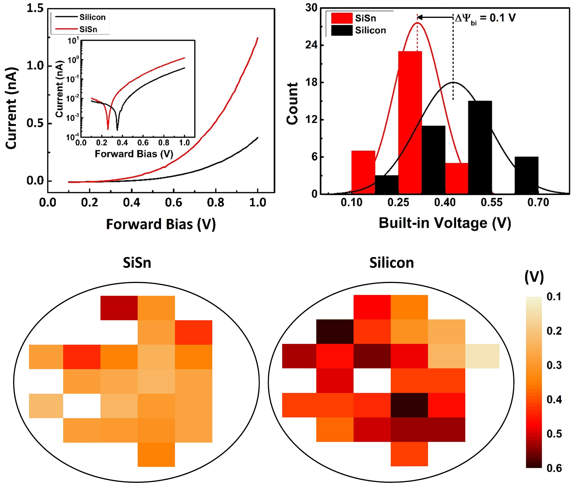
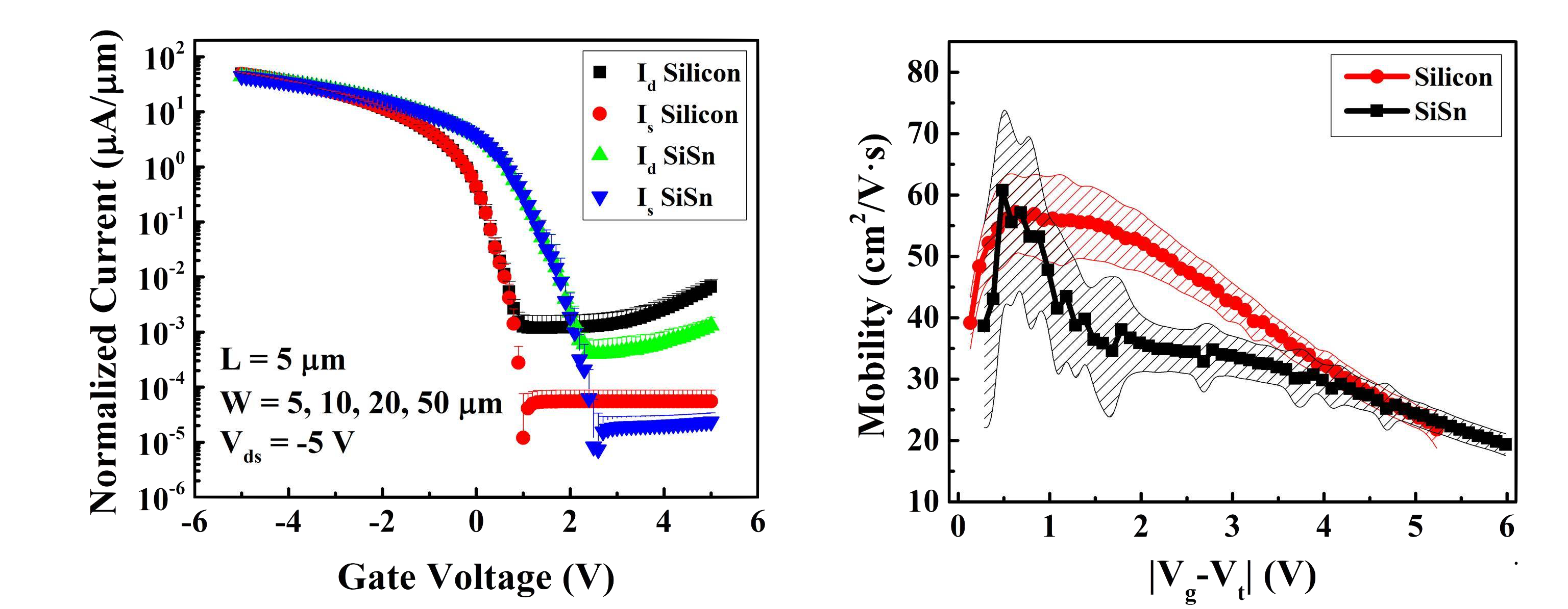
Because our theoretical model predicted a higher mobility for p-channel SiSn MOSFETs, due to a lower effective mass of the holes, we fabricated SiSn pMOSFETs and silicon p-MOSFETs for comparison. We observed an increase of 13.6% in the average field effect hole mobility for SiSn devices compared to silicon control devices. Further, our theory predicted a reduction in the bandgap of silicon lattice with incorporation of Sn. We verified this prediction experimentally by forming p-n junction diodes and by comparing the built-in potential and reverse breakdown voltages. We observed a reduction of 0.1 V in the average built-in potential, and a reduction of 0.2 V in the average reverse bias breakdown voltage, as measured across a 4 inch substrate.
So where to from here then?
The preliminary work done on SiSn has shown promise due to the inherent difference in electronic properties of the crystal compared to silicon. We have pioneered the experimental work on SiSn by fabricating SiSn wafers using thermal diffusion of tin into silicon. This research can be carried further by fabricating more SiSn channel based devices and studying various parameters such as SiSn-dielectric interface quality for various high-κ dielectrics, contact resistance for different silicidation conditions, CMOS circuit demonstration etc.
Drop on in
4700 KAUST, Ibn Sina Building (3),
Thuwal, Makkah
Saudi Arabia, 23955-6900
Give us a call
Office: +966-2-808-4450
Lab Phone: +966-2-808-0797
Contact online
Email: MuhammadMustafa.Hussain@kaust.edu.sa
INL: nanotechnology.kaust.edu.sa